Atomic Layer Deposition – Thin Layers Are a Big Thing

by Dr. Dirk Caspary
The article “Patent data shows the complexity of the semiconductor manufacturing market“, which was published in December of 2020, listed five semiconductor manufacturing equipment manufacturers among the top 20 patent owners in the technology field of semiconductor manufacturing. These patent owners were Applied Materials, ASM International, ASML, Lam Research, Tokyo Electron, and these owners are common household names in semiconductor manufacturing. Applied Materials, Lam Research, and Tokyo Electron are known as vendors for various semiconductor manufacturing equipment types, and ASML is known for its cutting-edge lithography tools.
What caught my attention was the presence of ASM International in the ranking among the top 20 semiconductor manufacturing patent owners, and the fact that ASM International ranked even better among the top 20 advanced semiconductor manufacturing patent owners. The ASM International annual report for 2020 states that more than half of ASM International equipment revenues come from atomic layer deposition (ALD) applications.
Atomic layer deposition is an amazing technology field, because – as the name already implies – it is about depositing layers that are so thin that thinner layers are hardly not possible: depositing layers which are only a few atomic layers or even a single layer thick. In semiconductor manufacturing, ALD processes are used for advanced transistors with layer stacks in transistor gate electrics, gate electrodes, or in the interconnects. Thus, let’s have a look at the ALD patent landscape.
The atomic layer deposition patents search
In order to obtain an overview on the atomic layer deposition patent landscape, a patent search was performed using the LexisNexis® PatentSight® business intelligence platform. The search is based on search terms, which commonly used for ALD, in a context of processes or apparatus adapted for the manufacture or treatment of semiconductor or solid-state devices or of parts thereof. In addition, stop terms are used in the database query to exclude unrelated unit processes and its manufacturing equipment.
The results
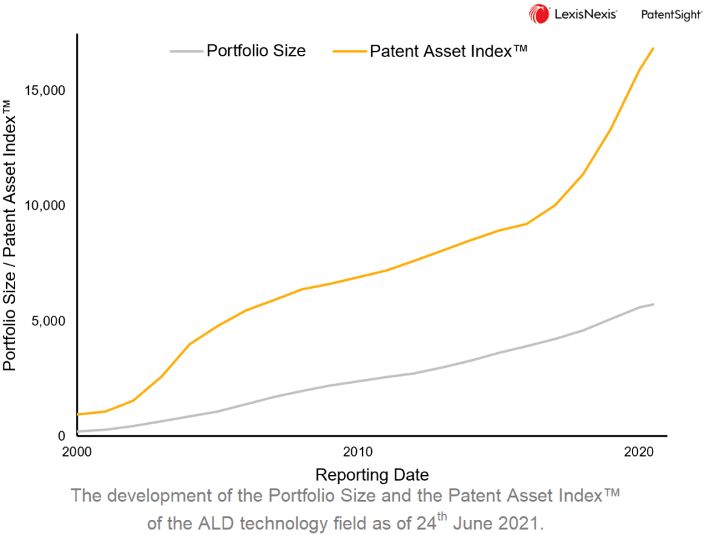
The figure shows the development of the Portfolio Size and the Patent Asset Index. The Portfolio Size is defined as the number of active patent families, and the Patent Asset Index measures the strength of a patent portfolio.
Whereas the Portfolio Size shows an almost linear growth rate since the year 2000, the Patent Asset Index shows a trend with could be roughly split into three periods: until 2005, between 2005 and 2015, and since 2016.
Interestingly, these periods appear to coincide with major developments in semiconductor manufacturing and its respective market introductions of commercial products.
For example, in comparison to the Portfolio Size development, the Patent Asset Index disproportionately increases until about the year 2005. This disproportionate increase shows that the underlying Technology Relevance of ALD patents has increased accordingly, which in turn is regarded as an indicator for significant research and development (R&D) activities during this period. Once these activities have calmed down, the high-k metal gate technology was introduced with the 45 nm process node in 2007, followed by the introduction of the 3-dimensional gate structures in 2012 which are commonly known as tri-gates or finFET.
Now, nine years later, we are apparently again in a very active atomic layer deposition R&D phase. The comparison with the last active R&D period suggests the assumption that the semiconductor industry is up to something, and the obvious guess would be the introduction of commercialised gate-all-around (GAA) transistor technologies in about a year’s time.
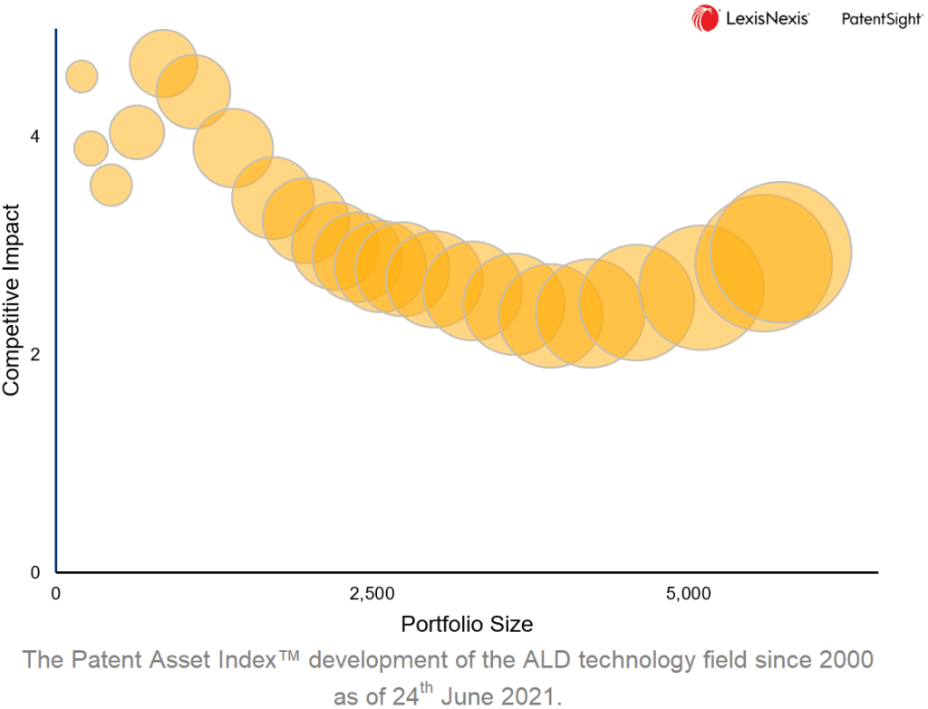
The figure above shows an alternative view on the portfolio strength trend measured by the Patent Asset Index which is equal to the product of the Portfolio Size and the average patent quality (Competitive Impact). In this figure, the Patent Asset Index development over time is plotted with respect to its two components, and the bubble size represents the Patent Asset Index.
Ignoring the Competitive Impact variations in the early 2000s, the figure shows up to 2016 the common rule of thumb that the average patent quality (Competitive Impact) declines as the Portfolio Size increases. Then, since 2017 we see a reversal of this general rule, and the average patent quality increases again.
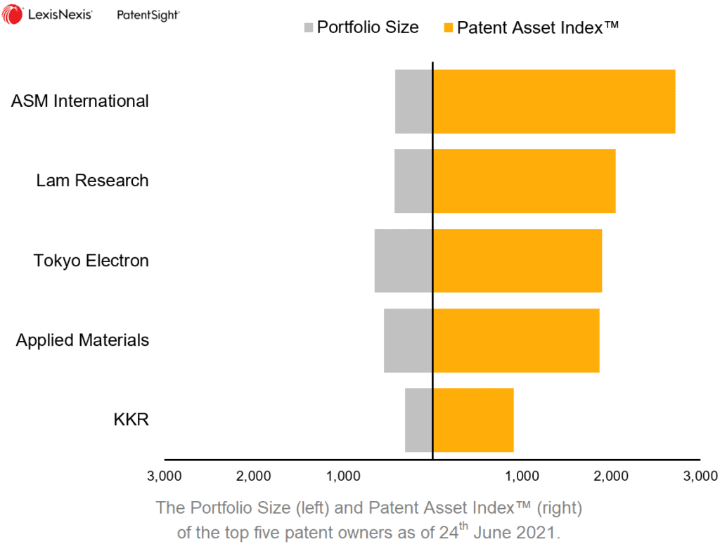
The figure shows the Portfolio Size and the portfolio strength measured by the Patent Asset Index for the top five patent owners. The top four patent owners Tokyo Electron, Applied Materials, Lam Research, ASM International are already known from the earlier mentioned article “Patent data shows the complexity of the semiconductor manufacturing market”. The fifth patent owner KKR is the ultimate owner of ALD patents originating from Hitachi and Kokusai Electric.
For the top four patent owners, the figure clearly illustrates the difference between a patent owner’s Portfolio Size in a technology field and the respective strength (Patent Asset Index) in that technology field.
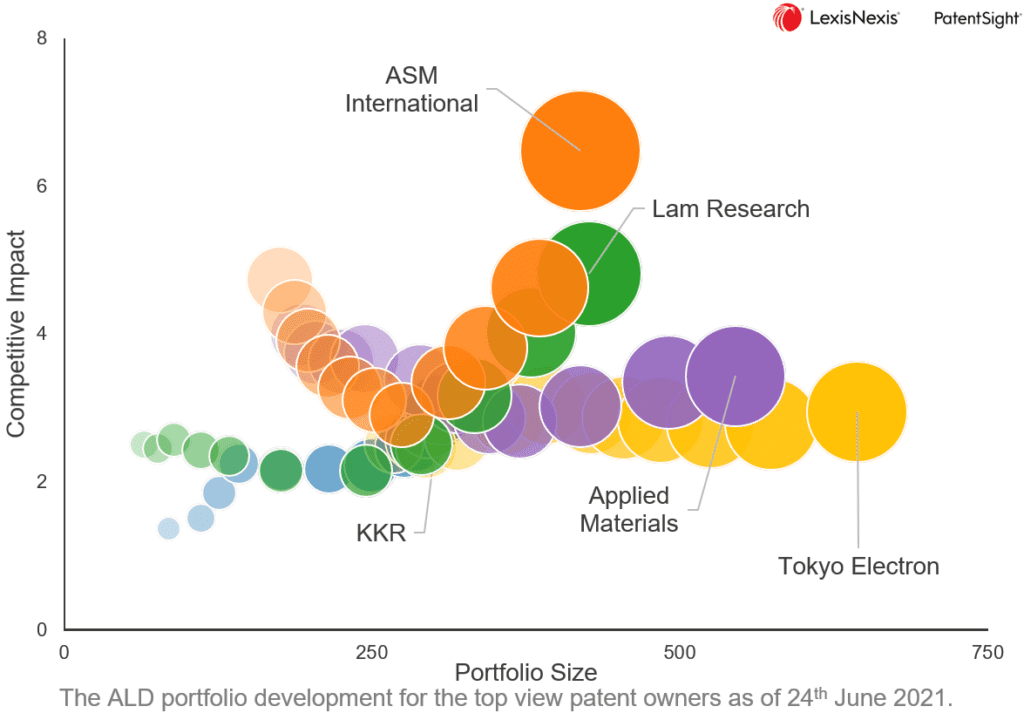
Focusing now on the last 10 years for the top five patent owners, a division among these patent owners is unveiled: While significantly increasing their respective ALD patent portfolios, ASM International and Lam Research have significantly increased the average patent quality (Competitive Impact) since 2017. In contrast, Applied Materials and Tokyo Electron cannot keep up with the average patent quality increase of their competitors. And at last, the ALD patent portfolio owned by KKR does not appear to be further actively developed.
The question that arises here is whether if patent information can give insights into what separates ASM International and Lam Research from Applied Materials and Tokyo Electron.
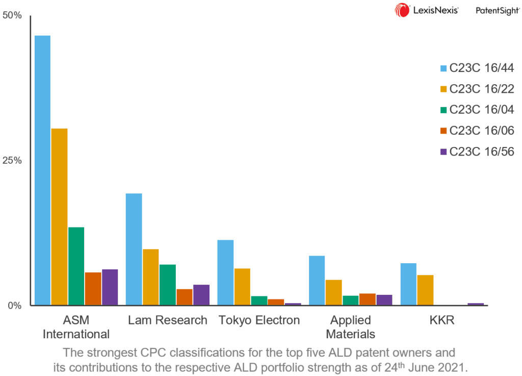
In order to differentiate the top five ALD patent owners, the top five CPC classifications were analysed, which are all sub-groups of the C23C 16/00 main group classifying “chemical coating by decomposition of gaseous compounds, without leaving reaction products of surface material in the coating”.
The figure shows the strongest five CPC main groups as the share of the total portfolio strength of the top five patent owners. As a reading example, all ASM International patents which are classified by the CPC sub-group C23C 16/44 or one of its sub-groups account for almost 50 % of the strength of ASM International ALD patent portfolio.
All top five patent owners have approximately the same ratio of the two sub-groups
- C23C 16/44 “characterised by the method of coating” and
- C23C 16/22 “characterised by the deposition of inorganic material, other than metallic material”
in common; but the third sub-group
- C23C 16/04 “coating on selected surface areas, e.g. using masks”
seems to differentiate ASM International and Applied Materials from the others. The absence of the C23C 16/04 sub-group for the KKR patents supports the earlier impression, that this ALD portfolio is not actively developed anymore.
Eventually, there is the question if the strength in the intellectual property realm is transformed into an actual business strength. Without being a stock markets expert, I looked at the relative stock price developments for ASM International, Lam Research, Applied Materials, and Tokyo Electron over the last decade. Not only that the overall development is impressive, but it also seems that the split between the companies resembles the split in portfolio strength.
Learn more about PatentSight and the Patent Asset Index.
Excellent data quality is the foundation of reliable analyses. Learn how PatentSight enhances patent data here.
See how to use the Patent Asset Index for patent portfolio benchmarking.